
A PCB-mount micro switch is not a generic three-pin component with a universal footprint. Before laying out copper, identify the exact terminal variant, confirm the manufacturer’s drawing, map COM/NO/NC, and leave enough space for the actuator and its full travel. For an OEM design, the board footprint, mechanical support, solder process, and electrical duty must be checked together.
This guide uses the LEMA KW10-0P as a product-specific example. It is a small snap-action switch with straight PCB terminals; the family also illustrates why terminal suffixes matter. Do not copy a footprint or solder profile from another KW10 variant without matching the exact drawing and controlled specification.
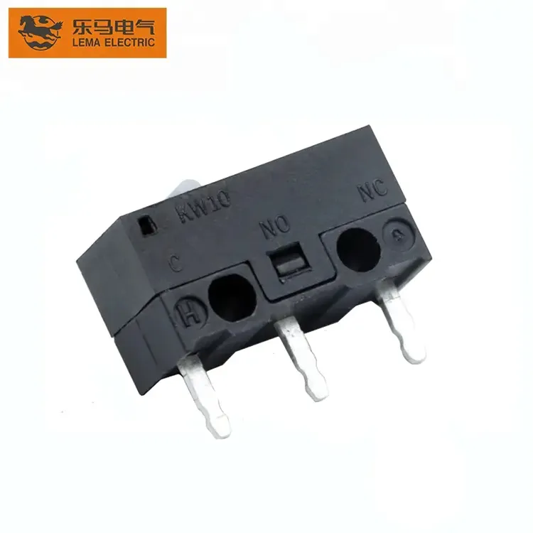
What makes a micro switch PCB-mountable?
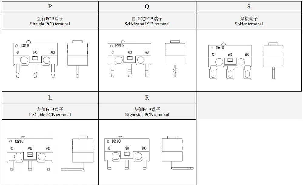
A PCB-mount switch has terminal geometry intended to enter or connect to a printed circuit board. That description alone does not tell you whether the part is through-hole, how much of the terminal is designed to be soldered, whether the switch body needs a separate support, or what board-hole dimensions to use. Product families may offer straight PCB pins, self-fixing pins, solder lugs, quick-connect tabs, and wire terminals. These are distinct interfaces, not interchangeable names for the same footprint.
For example, the KW10 terminal reference image distinguishes straight PCB terminals from a self-fixing PCB terminal and a solder terminal. The suffix and exact drawing determine which one is supplied. A straight pin may rely on the PCB and fixture to hold alignment during assembly; a self-fixing form may use a different pin shape. Neither should be assumed from a photograph of the switch top alone.
Start with the drawing, not a copied footprint
Download the dimensional drawing for the exact order code and record the drawing revision beside the PCB library part. Identify the switch’s mounting datum, terminal center coordinates, terminal width and thickness, case outline, actuator location, and any lever or plunger envelope. The LEMA KW10-0P product page provides product-specific references, including terminal and mounting-hole views. Use those dimensions rather than scaling an image in a browser.
Do not infer pin spacing from a rendered product image. Images can be resized, cropped, or intended only to show appearance. If the drawing is unclear, request a dimensioned drawing or sample before releasing the PCB. A useful internal library record includes the manufacturer, full model code, source drawing, revision/date, terminal type, hole pattern, and the engineer who checked the footprint.
| Footprint check | What to verify | Why it matters |
|---|---|---|
| Terminal pattern | Pin centers, count, terminal width and thickness | Prevents forced insertion, bent pins, or open joints |
| Hole and pad | Finished hole, copper annulus, solder mask, clearances | Supports the joint without reducing electrical spacing |
| Body outline | Case footprint, tolerance, nearby component keep-outs | Avoids collision and makes assembly repeatable |
| Actuator envelope | Plunger/lever position, movement path, access for the target | Prevents a board component or housing from blocking actuation |
| Orientation | COM/NO/NC side and board-side view | A mirrored footprint can reverse the circuit mapping |
Map COM, NO, and NC before routing
Many miniature snap-action switches expose common (COM), normally open (NO), and normally closed (NC) contacts. “Normally” describes the switch’s unactuated state. In a common SPDT arrangement, COM connects to NC while the actuator is released; when the switch operates, the moving contact transfers to NO. The exact contact form and pin layout must still be confirmed on the model drawing.
Build the schematic symbol and PCB footprint as a matched pair. A pin numbering convention is useful only if it agrees with the manufacturer’s view direction. Annotate whether the drawing is viewed from the actuator side, terminal side, or board side. Then use a continuity meter on a sample before power is applied: check COM-to-NC at rest, operate the switch, and check COM-to-NO. Do not assume that a familiar-looking three-pin pattern has the same left-to-right order as another supplier’s part.
For a controller input, decide whether the design needs an open circuit or closed circuit in its safe or idle state. Include the intended pull-up or pull-down, debounce strategy, and cable-fault behavior in the circuit review. A switch’s contact logic does not by itself provide a safety-rated function or diagnose a broken wire.
Allow for the switch body and actuator travel
The footprint is only one part of the mechanical interface. A target, cam, door, or lever must move the actuator far enough to change state without forcing the switch beyond its permitted travel. The assembly tolerance stack includes the PCB location, switch body variation, enclosure features, target position, and any bracket or fastener movement. Check both the earliest and latest possible actuation points—not only a nominal CAD model.
Leave clearance around the button or lever for its full operating path, and avoid placing a tall component where it can become an unintended stop. If the board is mounted in a vibration environment, do not rely on solder joints as the only mechanical restraint for repeated side loading. Add a bracket or housing support where the design requires it, while ensuring the support does not clamp the actuator or distort the switch case.
Review pre-travel, operating position, overtravel, release position, and differential travel from the exact product data. Do not transfer these values between actuator types. A roller lever, hinge lever, and pin plunger can produce different effective contact positions even when the internal switch family is related. If a mechanism uses a hard stop, set it so the application force cannot push the switch past its permitted mechanical limit.
Soldering: use the switch maker’s process limits
There is no safe universal solder temperature or dwell time for every PCB micro switch. Follow the instructions for the exact model and terminal construction. The temperature and exposure limits in another company’s micro-switch manual are not a specification for a KW10 switch. OMRON’s micro-switch technical guide illustrates why limits are model-dependent: it provides separate conditions for different terminal variants and warns against solder or flux reaching the case. Use the LEMA controlled specification for LEMA production.
For manual through-hole soldering, secure the board and switch so the terminals do not move while the joint forms. Heat the pad and terminal together, feed an appropriate amount of solder into the heated joint, then remove the solder and iron without pulling on the terminal. Avoid holding heat at the terminal longer than the approved process. Do not use the switch body as a fixture or press it into alignment while the joints are molten. Let the assembly cool without mechanical stress.
For wave or selective soldering, validate the board direction, preheat, flux application, contact time, and solder level on a representative assembly. Keep flux and cleaning solvent from entering an open switch. A process that appears acceptable from the underside can still allow residue to wick into the mechanism from the terminal side. Choose a compatible flux and cleaning process, and confirm whether the switch is sealed and washable before approving immersion or aggressive cleaning.
After soldering, inspect for insufficient wetting, bridges between adjacent terminals, disturbed pads, bent terminals, and flux residue. If the board will receive conformal coating, mask or protect the switch where required by its manufacturer. Coating that reaches moving parts or contact openings can change actuation or electrical behavior.
Check electrical duty separately from footprint fit
A part that fits the board is not automatically suitable for the load. Confirm AC and DC ratings separately, then check whether the actual load is resistive, capacitive, inductive, a lamp, or a motor. Startup current, switching frequency, voltage, ambient temperature, and the required electrical life all affect selection. A control input carrying a low-level signal also has different contact-reliability needs from a power circuit.
The LEMA KW10-0P page presents several electrical variants; use the rating that matches the exact ordered configuration and its test conditions. Do not combine the highest current from one row with the voltage from another row, and do not estimate a DC rating from an AC value. For inductive loads, evaluate the energy released when the circuit opens and use an appropriate suppression or relay arrangement where the circuit design calls for it. See the separate micro switch inductive-load guide for that topic.
For load selection, Panasonic’s switch terminology and use guidance explains why the actual current type and load matter. These manufacturer references are engineering context, not substitutes for the chosen switch’s own datasheet. For the general through-hole joint technique, SparkFun’s through-hole soldering tutorial is a neutral learning resource.
Production inspection and qualification
- Confirm the exact suffix, terminal type, drawing revision, and component orientation against the bill of materials.
- Inspect a first article for seating, pin alignment, solder wetting, bridges, and body damage.
- Measure continuity in the released and operated states, then confirm that the firmware interprets each state correctly.
- Cycle the real target through worst-case tolerance positions and verify reliable switching without overtravel.
- Test the intended load and switching rate under representative voltage, current, temperature, and enclosure conditions.
- Record the board revision, component lot, solder process, test fixture, and pass/fail criteria.
Qualification should include the assembled mechanism, not only a loose switch on a bench. A sample may click correctly while the production lever misses its operating point or the enclosure presses the button continuously. Verify repeatability after assembly and after the environmental exposures relevant to the end product.
Video: through-hole soldering basics
This SparkFun lesson demonstrates a general through-hole solder joint. Use it to understand the basic technique only; the switch manufacturer’s time, temperature, flux, and cleaning limits remain controlling for the selected model.

Frequently asked questions
Is every three-pin micro switch suitable for PCB mounting?
No. Confirm that the exact terminal variant is designed for the board and matches a dimensioned footprint.
Can I copy a footprint from another KW10 switch?
Only after confirming the same terminal suffix, pin pattern, orientation, and drawing revision.
Can I use an AC rating as the DC rating?
No. Use the published rating for the actual current type and load category; never infer a DC value from an AC row.
Can I use OMRON solder limits for a LEMA switch?
No. OMRON’s limits apply to its named models. Follow the controlled soldering conditions for the exact LEMA part.
What should be checked after soldering?
Inspect joints and residue, then verify COM/NO/NC continuity, actuation, clearance, and the assembled mechanism’s repeatability.
For related design topics, see the SPDT KW10 terminal and selection guide, the micro switch contact-resistance guide, and the micro switch product range.